
Format change
6×6 in → 6×12 in
announced Sept 8, 2026; pilot line by 2031, advanced-node production by 2033
Throughput recovered
~30%
175 wph → ~125 wph with stitching today; 12-inch mask restores single-shot on full 26×33 mm field
ASML 2026 EUV system plan
~65 Low-NA + ~10 High-NA
raised 2026 sales outlook to €43–45B in Q2 2026 results
The 30% Penalty Only a Bigger Mask Can Fix
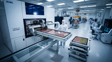
ASML's High-NA EUV scanner uses anamorphic optics that demagnify the mask 4× horizontally and 8× vertically. On a 6×6 inch reticle, the wafer-side exposure field collapses from the standard 26 mm × 33 mm to roughly 26 mm × 16.5 mm—about half the area. That half-field is a hardware constraint baked into the 0.55 NA projection optics; ASML executives have publicly stated there is no software or patterning workaround to restore it. To print a large AI accelerator die today, the scanner must expose the die in two stitched shots, and stitching costs High-NA wafer output: per ASML's announcement, scanner throughput falls from roughly 175 wafers per hour to about 125 wafers per hour, a ~30% productivity hit that scales with every High-NA tool shipped.
The 6×12 inch format—rectangular, twice as long in one dimension—is a physical prerequisite for High-NA EUV to deliver the wafer-per-hour economics the machines were sold to provide. Industry veteran Christopher Progler, cited in the Sept 8 coverage, called the shift a \"significant disruption\" affecting \"every tool involved in making masks.\" That is the operative sentence for investors: this is not a tweak, it is a re-tool.
The Consortium Locks the Schedule, and the Suppliers, In
Per the ASML and TSMC joint press releases dated September 8, 2026, the 'Large Mask Consortium' targets a 12-inch mask pilot line by 2031 and full High-NA lithography system readiness for advanced-node production by 2033. TSMC intends to begin High-NA EUV in high-volume manufacturing for advanced nodes starting in 2030—using current 6-inch masks first, then transitioning to 12-inch as the ecosystem catches up. Intel, which disclosed it has been running a parallel large-format mask effort for more than three years and has already processed over 1 million wafers with High-NA EUV on select Panther Lake (Core Ultra Series 3) layers at 18A in Oregon, joins the consortium with production experience to bring to the table.
- Samsung plans to use High-NA EUV for high-volume DRAM by 2028 with 6-inch masks and stitching, then adopt 12-inch once available—the most aggressive near-term user.
- TSMC's 2030 High-NA node entry on 6-inch masks is the bridging period that decides which suppliers get paid through 2032.
- Intel's prior 1M+ wafer High-NA production runs give it the only field data on pellicle survival and defect rates at source power—an underappreciated advantage in setting the new mask spec.
- Major High-NA EUV adopters, mask suppliers, and ecosystem partners 'expressed interest in joining' per the releases; the consortium is functionally a procurement signal to the supply chain.
| Company | High-NA HVM target | Format at start | Strategic read |
|---|---|---|---|
| TSMC (tsm) | 2030, advanced nodes | 6-inch (transitioning to 12-inch by 2033) | Bridge window determines who survives 2027–2032 |
| Intel (intc) | Now (18A / Panther Lake) | 6-inch → 12-inch | First-mover data; sets the spec; validates node economics |
| Samsung (ssnlf) | 2028, DRAM | 6-inch with stitching first | Most aggressive; will pressure-test pellicles and blanks |
| ASML (asml) | Scanner shipments ongoing | Both formats during transition | €380–400M per High-NA tool; long roadmap visibility |
Upstream: The Japanese Duopoly Refits; the Laggards Get Squeezed
Every supplier of EUV mask infrastructure—substrate, pellicle, photoresist, writer, inspection, metrology, and storage—has tools designed around 6×6 inch geometry. The new format forces a redesign across the entire stack, and the suppliers with the deepest pockets and the closest customer relationships have the easiest path. Per the Sept 8 coverage, the redesign list is explicit: mask blank substrate suppliers need new rectangular-format glass flatness and purity specs, pellicle manufacturers must develop films that protect the larger mask surface while withstanding higher EUV source power, and e-beam writers, defect inspection, overlay metrology, and handling/storage tooling each need format-specific redesign.
Hoya and AGC jointly control roughly 93% of the global EUV mask blank substrate market, a duopoly that has been consolidating for years. With their installed customer bases at every major mask shop and foundry, both have the engineering relationships to qualify new 6×12 inch substrates first. Shin-Etsu Chemical, which lists mask blanks alongside its semiconductor silicon and photoresist franchises, rounds out the materials layer; Tokyo Electron supplies coater/developer track tools that must be re-engineered for the new reticle handling. On inspection, Lasertec—the dominant EUV mask inspection specialist—and KLA must ship next-generation tools that can scan the larger field at throughput economics that make sense for the 2031–2033 ramp. And on pellicles, the Mitsui Chemicals partnership with ASML (signed in 2019, with commercial EUV pellicle production since 2021) is the only fully commercial source of EUV pellicles today—any 12-inch format pellicle for High-NA flows through them.
- Hoya: IT segment (mask blanks/photomasks/HDD glass) is a minority of revenue but the highest-margin piece—format leadership protects pricing through the transition.
- AGC: diversified conglomerate (glass, electronics, chemicals) where EUV blanks are a small fraction of revenue but the format switch keeps them inside the High-NA supply chain.
- Toppan: the world's premier merchant mask maker (now operating as Tekscend Photomask) with ~25% share of advanced photomask production for 3 nm and below—must refit its lines for 12-inch format to defend share.
- Mitsui Chemicals: the only commercial EUV pellicle source via its ASML partnership—12-inch pellicle qualification becomes a chokepoint for the entire industry's timeline.
- Lasertec: the EUV mask inspection leader with 59.2% TTM gross margin—its 12-inch inspection tool roadmap determines whether the 2031 pilot line can produce qualified masks.
- KLA: broad mask/wafer inspection and metrology—format-aware reticle inspection is an extension of existing platforms, with margin upside as the format ships.
- Shin-Etsu and JSR: photoresist and mask blank chemistry must be re-formulated for the new substrate flatness/purity profile—incumbents win by default.
- Tokyo Electron: coater/developer and track equipment must handle the larger reticle without throughput loss—format support is a precondition for tool refresh orders at the leading-edge fabs.
Downstream: Foundries Win the Long Game; Intel Holds the Only Production Data
For the foundries, the reset is unambiguously positive on a 1–3 year view: it converts a known 30% productivity penalty on AI die sizes into a recoverable throughput gain. TSMC is the most exposed to the penalty—its 2 nm and A12/A14 ramps face the largest AI die sizes—but the consortium's 2033 timeline gives it a 7-year bridge to amortize the existing 6-inch tool base. Intel, which announced on July 15, 2026 that Panther Lake (Core Ultra Series 3) layers on 18A had become the first high-volume logic product shipped with High-NA EUV, already has 1 million wafers of production data informing the consortium's pellicle, blank, and inspection specs—a quiet but real advantage when the new format must be qualified against existing 6-inch reference data.
Samsung is the outlier in timing: it is targeting High-NA EUV for high-volume DRAM by 2028, ahead of the consortium's 2031 pilot line, which means Samsung will run on stitched 6-inch masks for several years before 12-inch catches up. The implication for investors: Samsung's DRAM capex through 2027 carries a hidden throughput discount on every High-NA tool it installs, but its early adoption locks it into the format before competitors can establish alternative standards. ASML, for its part, raised its 2026 total net sales outlook to €43–45 billion with a 54–56% gross margin in its July 15, 2026 Q2 results—Q2 EUV system sales alone were €3.8 billion including one High-NA system—and the consortium announcement lengthens the visibility of the High-NA install base well into the late 2030s.
Short-Term (Days–Quarters): The Supply Chain Reads the Signal
The immediate market read is a procurement signal. Customers (TSMC, Samsung, Intel, IMEC) will start placing 12-inch mask ecosystem RFIs and qualification orders within the next 6–12 months; suppliers with a credible 6×12 inch substrate or pellicle roadmap will get preferred-supplier status in those negotiations. Suppliers without one will face the choice of expensive catch-up R&D or a multi-year exclusion from the High-NA ramp. Investors should track: Hoya and AGC substrate capex guidance in their next earnings cycles, Mitsui Chemicals' pellicle capacity commentary, and Lasertec's next-generation EUV mask inspection tool shipment timing.
For ASML and TSMC, the immediate term is mostly optics: the announcement lengthens the High-NA revenue curve into the 2030s but does not change 2026–2027 system shipments. The bigger read is that TSMC publicly reversing its prior skepticism of High-NA EUV—signaled by the consortium co-leadership and the 2030 HVM target—removes a key overhang on ASML's 2028+ High-NA install assumptions.
Long-Term (1–3 Years): Format Lock-In Reshapes the Mask Industry
By 2031–2033, the mask industry splits cleanly into '12-inch qualified' and '6-inch only' suppliers. The former ride the AI accelerator cycle into a multi-year capacity build; the latter get relegated to trailing-edge logic, mature DRAM, and non-leading-edge packaging applications. With the EUV mask blank market projected to reach roughly $1.3 billion by 2035 (a ~13% CAGR from 2026's ~$300 million base per multiple industry estimates) and the broader photomask market growing at a 4–7% CAGR through 2031, the 12-inch format reset is not a market expansion—it is a market reshuffle. The Japanese duopoly and the established mask-tool vendors capture the value; new entrants face the highest barrier to entry in the photomask industry's history.
For Intel, the long-term read is the most consequential: being the only foundry with High-NA EUV in volume production today, and being inside the consortium setting the next format, gives 18A and 14A a credibility tailwind that the company's 2024–2025 narrative did not have. The risk is execution—Intel's Panther Lake volume must clear its early-yield questions—but the strategic positioning improves meaningfully with this announcement.
The Thesis: A Format Reset, Not a Market Reset
ASML and TSMC did not announce a new chipmaking breakthrough on September 8, 2026—they announced a procurement commitment. But the commitment is large enough to reshape who makes money from photomasks over the next decade. The 30% High-NA throughput penalty that was a known cost of doing business on AI dies becomes a recoverable gain for anyone whose mask infrastructure can run on 6×12 inch format. The Japanese substrate and pellicle duopoly—Hoya, AGC, Mitsui Chemicals—and the established mask-tool vendors—Lasertec, KLA, Toppan via Tekscend, Tokyo Electron, Shin-Etsu, JSR—emerge with the strongest positioning. Smaller mask infrastructure challengers without the capital or customer relationships to retool get frozen out of the leading edge.
The risks to this thesis are concrete: (1) the 2031 pilot line slips, leaving the 6-inch format as the binding constraint longer than planned; (2) pellicle yield at 12-inch format with High-NA source power proves harder than expected, gating the 2033 readiness date; (3) alternative architectures (multi-patterning without High-NA, double-patterning, or competing lithography approaches) gain ground before 12-inch masks reach HVM economics. None of these are base-case scenarios today—but all are the variables that will determine whether the 30% throughput recovery actually arrives in the early 2030s or slides later.
Investable Takeaways
- Consortium locks High-NA HVM roadmap through 2033, extending the visibility of the €380–400M-per-tool install base beyond prior 2028 assumptions.
- Q2 2026 results raised 2026 sales outlook to €43–45B (Q2 EUV sales €3.8B incl. one High-NA); the format reset removes the TSMC adoption overhang on 2028+ High-NA shipments.
- Near-term (days–quarters): minimal system-shipment change; long-term (1–3 years): longer revenue tail and stronger High-NA pricing power.
- 2030 High-NA HVM target on advanced nodes reverses prior public skepticism and removes a key competitor narrative risk.
- 12-inch format eliminates the 30% stitching penalty on its largest AI dies (A12/A14 era), protecting gross margin (64.2% TTM) on the highest-value wafer mix.
- Near-term (days–quarters): no P&L impact; long-term (1–3 years): throughput recovery and lower cost-per-die on leading AI accelerators.
- Already shipping high-volume Panther Lake (Core Ultra Series 3) on 18A with High-NA EUV since July 15, 2026—only foundry with real production data to set 12-inch specs.
- >1 million High-NA wafers processed to date gives Intel outsized influence on pellicle, blank, and inspection qualification for the 2031 pilot line.
- Near-term (days–quarters): stock already moved +9.6% on the day on broader AI sentiment; long-term (1–3 years): format leadership supports 18A/14A credibility.
- Co-leader of the EUV mask blank duopoly (~34% share, ~93% combined with AGC) with installed customer relationships at every leading-edge mask shop.
- 12-inch substrate qualification timeline becomes a moat—first qualified substrate vendor captures the 2031 pilot line and 2033 HVM economics.
- Near-term (days–quarters): watch substrate capex commentary in next earnings; long-term (1–3 years): pricing power protected through the format transition.
- Largest single share of the EUV mask blank market (~59% per industry estimates); format transition solidifies rather than disrupts its position.
- Diversified revenue base (glass, electronics, chemicals) absorbs the R&D cost of 12-inch substrate development more easily than pure-plays.
- Near-term (days–quarters): minimal headline impact; long-term (1–3 years): retained leadership in the largest mask blank format in history.
- Only commercial source of EUV pellicles today via its ASML partnership (since 2021); 12-inch pellicle qualification is a chokepoint for the entire 2031–2033 timeline.
- Offsetting risk: EUV pellicle is a small fraction of a ¥2.3T-revenue diversified chemicals portfolio, so the upside is incremental rather than transformative.
- Near-term (days–quarters): format announcement is a positive read; long-term (1–3 years): single-supplier leverage on a critical consumable.
- Dominant EUV mask inspection specialist with 59.2% TTM gross margin; its 12-inch inspection tool roadmap effectively sets the pace of mask qualification.
- Format transition forces every existing EUV mask inspection install base to be re-tooled—Lasertec captures the replacement cycle as the only qualified supplier.
- Near-term (days–quarters): minimal revenue impact; long-term (1–3 years): strongest leverage in the mask-tool layer to the format reset.
- Broad mask/wafer inspection and metrology (TTM revenue $13.6B, gross margin 61.3%) with format-aware reticle inspection as an extension of existing platforms.
- KLA's installed base at every leading-edge fab means the 12-inch format drives a refresh cycle in inspection and metrology tools starting in 2027–2028.
- Near-term (days–quarters): no order impact; long-term (1–3 years): mask-inspection refresh revenue layer on top of an already growing AI-driven tool demand.