
SK Hynix Q2 2026 revenue
KRW 79.32T
$54.55B; +257% YoY, reported Jul 29, 2026
SK Hynix Q2 2026 operating margin
76%
Operating profit KRW 60.54T, record high
Intel Ohio One original capex
$28B
Licking County, OH; originally targeted 2025, now 2030–2031
Intel CHIPS Act direct funding (Ohio)
$7.865B
Awarded Nov 2024; $1.5B earmarked for the Ohio One campus
Intel Foundry Q2 2026 operating loss
($2.09B)
36% loss margin; external revenue only $293M
SK Hynix target US investment by 2030
$45B+
Indiana packaging + Ohio front-end, per CEO Kwak Aug 2026
Ohio's empty $28B shell finally gets a paying tenant
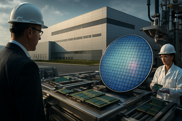
SK Hynix and Intel are in talks for a deal that would put memory wafers on US soil for the first time — and the Reuters exclusive on September 16, 2026 lays out two specific shapes the agreement could take: [SK Hynix] would either lease part of [Intel]'s long-planned Ohio One campus, or form a joint venture with [Intel] and major cloud firms to underwrite the buildout. Both sides have left the door open since [SK Hynix] walked back an earlier outright-acquisition story on July 22, and Ohio Senator Jon Husted publicly confirmed the talks weeks later, but neither company has signed anything yet.
The Ohio site is the deal's natural anchor. [Intel] broke ground in September 2022 on what was originally framed as a $20B project, then raised the planned investment to more than $28B in March 2024 for two leading-edge fabs in Licking County — a campus sized for roughly eight fab modules in total. Construction has been pushed to 2030–2031 after repeated delays, the US Department of Commerce has awarded [Intel] up to $7.865B in CHIPS Act direct funding (with $1.5B explicitly earmarked for the Ohio One project), and the first module is slated to produce the 14A node and other future [Intel] processes. Reuters says it could not determine which chip types — DRAM, NAND, or HBM — [SK Hynix] would actually produce there, but the front-end memory footprint is the prize: a US front-end fab lets [SK Hynix] skip the back-end-only model it is currently building in Indiana.
Why SK Hynix is renting, not building
[SK Hynix] is not acquiring [Intel]'s Ohio fab, despite the breathless July headlines from JoongAng Daily. The cleaner trade for both sides is a lease or operating partnership: [SK Hynix] inherits a permitted, partially-built, US-funded shell; [Intel] keeps the asset on its books, keeps its CHIPS Act money, and recovers some of the carrying cost on a campus whose first wafer was supposed to ship in 2025. The 1.2-million-pyeong site is large enough for eight fab modules, more square footage than [SK Hynix] could realistically greenfield in five years, and Ohio's power, water, and permitting groundwork is already done.
The economics push [SK Hynix] toward renting too. [SK Hynix] posted KRW 79.32 trillion in Q2 2026 revenue (up 257% year-over-year) and a 76% operating margin — a once-in-a-cycle windfall, but one tied directly to AI-driven HBM pricing that history suggests will normalize. Spending tens of billions of dollars on US land and a greenfield cleanroom would convert that windfall into a multi-decade depreciation anchor at exactly the wrong moment. Leasing a half-built [Intel] campus lets [SK Hynix] reserve a US footprint, qualify for incremental CHIPS funding, and lock in customers like the cloud hyperscalers mentioned in Reuters's venture scenario — without writing the capex check itself.
- [Intel] Q2 2026 net loss of $11.03B and Intel Foundry losses of $2.09B make a paying memory tenant more attractive than ever — Apple agreed in May 2026 to use Intel 18A-P, but external Foundry revenue is still only $293M a quarter
- The same Trump-administration logic that converted $8.9B of CHIPS Act and Secure Enclave grants into a 9.9% [Intel] stake last August wants visible US memory capacity; a [SK Hynix] lease delivers it without a new federal outlay
- [SK Hynix]'s other US bet, the $3.87B West Lafayette Indiana packaging plant, is on track for cleanroom opening in October 2028 and HBM mass production in H2 2029 — Ohio would slot in alongside, not replace, that roadmap
The CHIPS Act playbook pivots from logic to memory
Through2025 the CHIPS Act story was a logic story: [Intel]'s Ohio and Arizona fabs, Samsung Electronics's $17B Taylor, Texas campus (now planned to add a second fab by 2030 inside a $55B Central Texas investment), and Micron's Idaho and New York DRAM clusters built to qualify for federal grants. The September 16 [SK Hynix]-[Intel] talks are the first time the federal framework is being actively redirected toward a foreign memory leader with no US-listed equity, no US board representation, and no CHIPS Act award of its own — beyond the $450M in direct funding SK Hynix already received for advanced packaging in 2024.
What makes the deal structural, not transactional, is the way it fuses [Intel]'s logic process technology with [SK Hynix]'s memory dominance. Reuters reports that [SK Hynix] is also evaluating [Intel] Foundry for next-generation HBM4E base dies, alongside TSMC's12nm-class process that currently supplies the logic layer under the HBM4 stack. If [SK Hynix] anchors HBM4E base dies at [Intel] 18A or 14A while also operating memory fabs at Ohio, the CHIPS-funded [Intel] campus becomes the substrate for the entire HBM stack — base die plus memory — instead of a logic-only asset. That is a quietly radical reorganization of who builds what in the US.
| Project | Owner | Total capex | First production | Product mix |
|---|---|---|---|---|
| Ohio One campus | Intel (with SK Hynix in talks) | $28B+ | 2030–2031 (mod1) | Logic 14A + possible DRAM/HBM/NAND |
| West Lafayette, Indiana | SK Hynix | $3.87B | H2 2029 HBM | Advanced packaging only |
| Taylor, Texas (Fab 1) | Samsung Electronics | $17B | End of 2026 | Leading-edge logic |
| Taylor, Texas (Fab 2) | Samsung Electronics | Part of $55B Central TX | 2030 | Logic |
| Boise, Idaho (ID1/ID2) | Micron | Part of $250B+ plan | 2027 (ID1) | Leading-edge DRAM/HBM |
| Clay, New York | Micron | Part of $250B+ plan | Mid-2027 | DRAM/HBM |
Upstream: lithography, etch, and chemicals get a new US memory customer
Front-end memory fabs are tooling-intensive in a way packaging fabs are not. A greenfield DRAM/HBM module needs immersion and EUV lithography, deposition and etch clusters, and a continuous drumbeat of advanced chemicals — a stack where ASML, Applied Materials, Lam Research, Tokyo Electron, and KLA split the wallet. An [SK Hynix] lease at Ohio converts what would have been a 100% [Intel] logic tool order book into a hybrid memory-plus-logic order book starting in 2027–2028, exactly when the equipment complex has been guiding to a digestion year. [ASML] booked EUR 9.33B in Q2 2026 revenue alone, and [Tokyo Electron]'s fiscal Q1 (June 2026) sales hit JPY 732B — both up sharply year-over-year — so the marginal question is whether an Ohio memory tenant accelerates or merely smooths the next leg of demand.
The nearer-term tie-up is already public. [Applied Materials] signed a long-term R&D partnership with [SK Hynix] in March 2026 at its new EPIC Center in Silicon Valley, focused on next-generation DRAM, HBM, and 3D advanced packaging — the same set of problems a US memory fab will need solved. [SK Hynix]'s procurement pipeline has historically centered on Korean and US suppliers, and the supply-chain lift is explicitly downstream of any Ohio deal: roughly 100 Indiana packaging suppliers are already under evaluation, and Ohio would extend that footprint to front-end tools.
Latest quarterly revenue — equipment companies most exposed to new US memory fabs
Quarterly revenue (USD billions), most recent reported quarter. Source: company earnings releases /10-Q filings.
Unit: USD billions
ASML Q2 2026
EUR 9.33B at ~1.09 USD/EUR
10.2
Tokyo Electron FY27 Q1
JPY 732B at ~155 USD/JPY
4.7
Applied Materials fiscal Q3 2026
FY Q3 ended Jul 27, 2026 (estimate)
7.4
Lam Research fiscal Q4 2026
FY Q4 ended Jun 28, 2026 (estimate)
5.3
Downstream: the HBM oligopoly gets its first US anchor
The September 16 deal does not break the HBM oligopoly in the near term. [SK Hynix] still controls roughly 50% of the global HBM market, with [Samsung Electronics] climbing toward 33% in Q2 2026 (up from 21% in Q1) after passing Nvidia HBM4 qualification, and [Micron] holding roughly a fifth. Reuters's reporting makes clear that the Ohio site will not produce wafers until at least 2028–2030 — long after the current HBM4 ramp, and possibly not in time to materially affect the HBM4E cycle that follows. Pricing power for HBM4 in2026 and 2027 is therefore unchanged; what changes is the geography of incremental capacity.
[Micron] is the most exposed incumbent. Its Idaho and New York fabs are funded by a $250B+ US capex plan through 2035 and are explicitly being built to address HBM domestic-content requirements from US hyperscalers. A [SK Hynix] Ohio fab directly into the same customer wallet means [Micron] loses some of the 'only US option' premium it has been trading on since the Trump administration expanded the federal stake in domestic memory production in June 2025. [Samsung Electronics] is less exposed — its $17B Taylor campus and follow-on Fab 2 are logic-focused, not memory — but loses the HBM4 narrative advantage if [SK Hynix] can credibly deliver US-made HBM at scale inside Nvidia's Vera Rubin roadmap window.
What changes in days versus what changes in years
In the next several quarters, the deal's market impact runs through three near-term readouts: an Ohio site announcement (likely Q4 2026 or Q1 2027 given that the two sides have not begun formal negotiations), incremental disclosure on the HBM4E base-die decision at [Intel]18A, and any signal on which cloud firms — Reuters names them generically — would anchor the joint-venture scenario. Each is a real catalyst for [SK Hynix], [Intel], and the equipment complex, but none changes unit volumes until 2028 at the earliest.
Over a1–3 year horizon, the structural implications are larger. A signed Ohio deal would harden the US government's quiet pivot from funding logic to underwriting memory, force [Micron] and [Samsung Electronics] to either accelerate their own US memory ramps or concede the 'Made in USA' HBM premium, and create a captive US customer base that [SK Hynix] can serve without exporting finished stacks from Korea. Risks cluster around three points: the deal never closes because the parties cannot agree on economics; the federal government withholds CHIPS-related approvals because of foreign-ownership sensitivities around a $45B+ Korean footprint; and the Ohio site remains structurally delayed past 2031, leaving [SK Hynix] carrying lease costs on an asset that ships no wafers.
- [SK Hynix]'s H1 2026 cumulative revenue of more than KRW 131T and HBM Q2 2026 revenue of KRW 9.4T mean the company can fund an Ohio lease from internal cash (KRW 54.3T at the end of Q1) without diluting shareholders — a structural advantage versus [Micron]'s debt-funded $250B US plan
- [Intel]'s $7.865B CHIPS Act funding is milestone-linked; an [SK Hynix] lease that accelerates first-wafer-out dates directly de-risks [Intel]'s 2030–2031 timetable and the warrant trigger tied to its foundry ownership
- The deal sets up a 2027 catalyst chain — formal JV announcement, hyperscaler anchor naming, base-die sourcing decision — that will move the equipment complex first, the memory trio second, and [Intel] Foundry third
Investable names most exposed to a SK Hynix–Intel Ohio memory fab
- An Ohio front-end fab stretches SK Hynix's HBM lead into a US-anchored one, qualifying future output as 'Made in USA' from ingot to stack for Nvidia, AMD, and US hyperscalers
- Q2 2026 operating margin of 76% and KRW 54.3T cash give the balance sheet capacity to absorb lease economics without diluting equity — the structural advantage over [Micron]'s debt-funded US plan
- Long-term thesis stays in place even if the deal slips: the existing $4B Indiana packaging facility still reaches first HBM mass production in H2 2029 with no Ohio dependency
- A paying Ohio tenant cuts Intel Foundry's $2.09B quarterly burn by sharing fixed costs on the Licking County shell — but external Foundry revenue was only $293M in Q2 2026, so memory has to scale fast to move the needle
- The HBM4E base-die evaluation puts [Intel] 18A and 14A in front of the fastest-growing AI silicon category; winning that socketpulls ~$1–3B of incremental foundry revenue into 2027–2028, even before Ohio wafers ship
- Q2 2026 GAAP net loss of $11.03B and -19.8% net margin cap any near-term multiple re-rating — the deal helps the story, not the print
- A [SK Hynix] Ohio fab erodes Micron's 'only US HBM source' premium by adding a second domestic front-end memory footprint before Micron's first New York wafer ships in mid-2027
- Micron's $250B+ US capex plan was sized against a tighter US-content oligopoly — that plan now competes with subsidized Korean capacity on US soil, putting downward pressure on long-run HBM pricing
- Near-term the thesis still works on Q3 FY2026 results (revenue $41.46B, operating margin 80%), but 2028–2030 US HBM supply is materially less scarce than the buy-side currently models
- An Ohio front-end memory fab adds EUV and immersion lithography demand on top of [Intel]'s logic roadmap — incremental2027–2029 tool orders sit ahead of the consensus digestion year
- Memory fabs buy different nodes than logic fabs; an [SK Hynix] lease widens ASML's TAM beyond the [Intel]/TSMC logic duopoly it has been over-indexed to
- Q2 2026 revenue of EUR 9.33B shows the order book is healthy before any Ohio upside — the deal is incremental, not required, for the next-year thesis
- [SK Hynix] is already a founding partner at Applied's EPIC Center for HBM materials and 3D packaging — an Ohio front-end fab converts that R&D partnership into a US-side tool pipeline
- Deposition and etch gear for memory is higher-mix than for logic, lifting Applied's content per wafer versus a pure-[Intel] logic shell
- Near-term read: Applied's fiscal Q3 2026 results (quarter ended Jul 27, 2026) frame the print before any Ohio news lands
- Memory etch intensity is structurally higher than logic — an Ohio memory tenant lifts Lam's content per wafer versus a pure-Intel logic scenario
- Fiscal Q4 2026 results (quarter ended Jun 28, 2026) carry the next near-term print; any incremental Ohio disclosure around that release is a positive catalyst
- Risk: if the deal slips past 2027, the boost lands in a digestion year — direction is right, timing is binary
- Coater/developer and single-wafer etch systems are memory-essential — Tokyo Electron's US-lite footprint gains a credible second US memory customer alongside [Micron]
- FY27 Q1 (June 2026) revenue of JPY 732B marks the recovery from the FY26 H1 trough, and an Ohio decision in 2027 would slot into the next capex up-cycle
- Trade is OTC ADR-driven with thin float — sizing matters, and direction depends on the deal formally closing